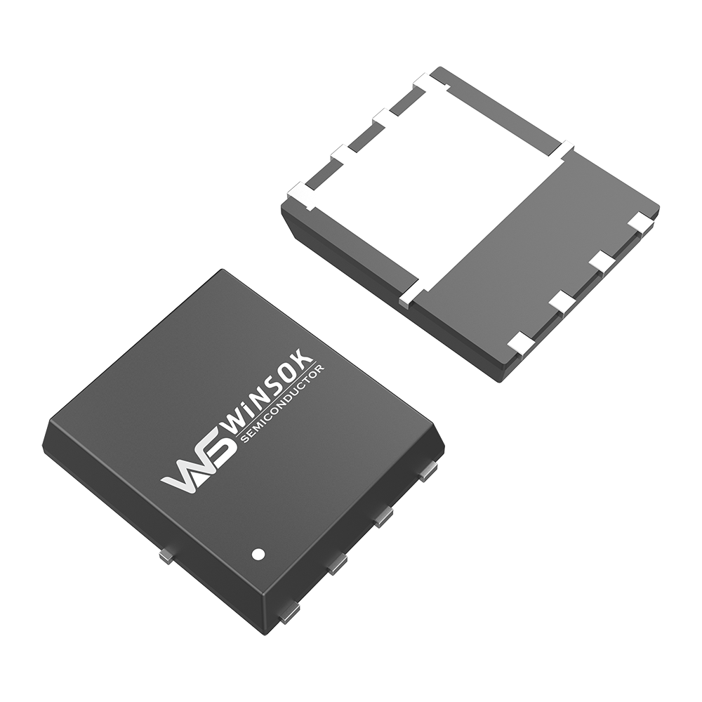
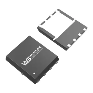
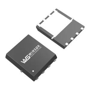
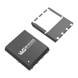
The voltage of WSD19N10DN56 MOSFET is ±100V, the current is 15A/-12A, the resistance is 100mΩ, the channel is N+P-channel, and the package is DFN5X6-8L.
What are the main channel specifications of the WSD19N10DN56 MOSFET?
The WSD19N10DN56 features a complementary N+P-channel configuration. The N-channel supports a drain-source voltage (VDS) of 100V and continuous drain current (ID) of 15A. The P-channel supports a VDS of -100V and a continuous current of -12A.
What is the typical on-resistance (RDS(ON)) value?
For the N-channel, the typical RDS(ON) is 100mΩ (110mΩ maximum) when measured at a VGS of 10V. For the P-channel, the typical RDS(ON) is 150mΩ (180mΩ maximum) at a VGS of -10V.
What type of package does this MOSFET use?
The device is housed in a compact, low-profile DFN5X6-8L surface-mount package, which provides excellent heat dissipation and a small board footprint.
What are the typical gate charges and input capacitances (Ciss) for both channels?
The input capacitance (Ciss) is 450pF for the N-channel component and 700pF for the P-channel component, offering optimized switching characteristics.
Which target systems commonly integrate the WSD19N10DN56?
It is widely applied in consumer and industrial systems such as E-cigarettes, wireless chargers, electric motors, drones, medical equipment, car chargers, controllers, digital products, small household appliances, and various consumer electronics.
 Olukey