Engineered for high thermal performance, low switching loss, and extreme dependability under harsh vehicle operating conditions.

Modern Advanced Driver Assistance Systems (ADAS) have transitioned from simple localized driver aids to complex, centralized high-performance computing (HPC) domains. With Level 2+ to Level 5 autonomous driving architectures packing heavy AI coprocessors, HD cameras, LiDAR (Light Detection and Ranging), and high-frequency radar units, power distribution networks must remain flawless.
In these environments, custom MOSFETs are the bedrock of electrical power units, protection systems, and switching converters. Standard commercial components fail to withstand the high thermal gradients, voltage spikes, and dynamic stresses characteristic of automotive power rails. Engineers require custom solutions optimized for ultra-low drain-to-source on-resistance ($R_{DS(ON)}$), high safe operating areas (SOA), and low thermal resistance ($R_{\theta JC}$) to minimize heat generation.
"As autonomous compute loads scale upwards of 100W to 500W, power conversion efficiency within the central ADAS controller becomes the primary constraint. Custom packaging and trench gate structures are no longer options; they are system prerequisites."

Our comprehensive selection of power MOSFETs provides micro-level power management across distinct ADAS functional subsystems.
LiDAR systems require extremely rapid, high-peak-current switching (nanosecond rise times) to generate optical pulses for 3D mapping. Custom medium-voltage MOSFETs (40V to 100V) in compact DFN3X3 or wafer-level packages minimize stray inductance, ensuring sharp pulse edges and accurate spatial resolution.
Millimeter-wave radar systems demand low-noise, high-transient response power rails. Our low-voltage N-channel and P-channel MOSFETs act as synchronous rectifiers and high-speed switches in multi-phase buck converters, keeping ripples down to microvolts to prevent RF signal degradation.
When high-current power buses boot, severe inductive kickbacks can burn sensitive computing processors. Utilizing low-resistance MOSFETs as high-side smart switches provides robust reverse battery protection and overvoltage clamping, vastly exceeding standard diode setups.
Pioneering the transition toward smart, integrated power devices that redefine density, speed, and efficiency standards.
The future of automotive power lies in higher levels of integration and smart diagnostics. WINSOK’s research roadmap is intensely focused on bringing "intelligent" features directly into the silicon of custom MOSFETs. Rather than relying on external sensors that add cost and board footprint, future generations will feature integrated temperature and current-sensing elements on-die, allowing microsecond-level fault detection inside ADAS computers.
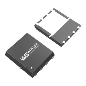
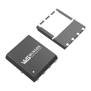
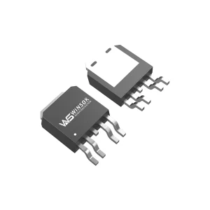
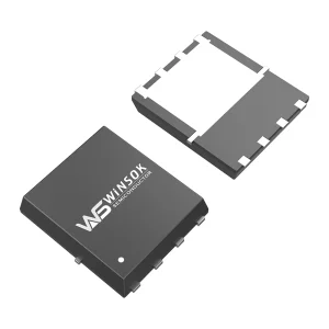
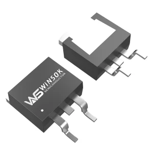
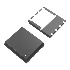
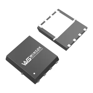
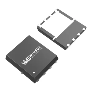
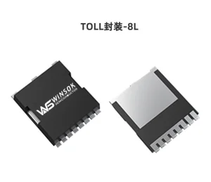
Simultaneously, we are scaling package configurations to match the aggressive miniaturization demands of modern vehicle architectures. As system boards compress, our package development is shifting toward next-generation PDFN (Power DFN) and TOLL (TO-Leadless) packaging. The TOLL format reduces board footprint by 30% compared to traditional D2PAK housings while improving thermal performance, facilitating high-current delivery up to 300A in high-voltage ADAS domain controllers.
| ADAS Component | Key Parameter Requirement | Preferred Package Option |
|---|---|---|
| LiDAR Laser Diode | Ultra-low gate charge ($Q_g$) | DFN3X3-8, DFN2X2 |
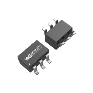
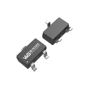
| Surround-View Cameras | Extremely small footprint | SOT-23, SOT-363, DFN2X2 |
| Radar Processing Unit | Low-frequency thermal cycling | DFN5X6-8L, SOP-8 |
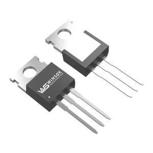
| Main Compute Engine (ECU) | High current density & low $R_{DS(ON)}$ | TOLL-8L, TO-252, TO-263 |
Hongkong Olukey Industry Co., Limited manages a highly sophisticated semiconductor fabrication ecosystem. Leveraging advanced factory automation and smart manufacturing (Industry 4.0), our partner wafer fabs and packaging lines operate under rigid electrostatic discharge (ESD) and environmental controls.
Our factories employ fully automated optical inspection (AOI) and X-ray imaging for every wafer batch. This ensures that micro-cracks, voiding in solder joints, or package misalignments are instantly caught and quarantined. For global automotive suppliers, this level of quality management translates directly into lower failure rates, minimizing warranty liabilities and field recalls.
Factory Capabilities: More than 600 models in active production across 40 specialized packaging lines. Robust resource buffer plans ensure scaling capacities can absorb high seasonal demands from the tier-1 automotive sector without delivery delays.





HONGKONG Olukey INDUSTRY CO., LIMITED is a premier global solution provider focusing on the overall architecture of electronic components. We design, manufacture, and distribute three major categories of high-tech products:
Relying on direct supply agreements and strategic partnerships with global original manufacturers, we support top-tier firms in automotive electronics, military hardware, smart energy, IoT systems, and medical diagnostics.

Over the years, Olukey Industry has built a reputation for consistency, engineering expertise, and quality-first support. We serve as a strategic partner to manufacturers, providing engineering design-in support, rapid prototyping, and scalable volume production.
Our WINSOK MOSFET range spans 15V, 20V, 30V, 40V, 60V, 80V, 100V, 120V, 150V, 200V, 250V, 300V, 400V, 500V, 600V, and 650V options. These are packaged in industry-standard forms, including DFN3X3-8, DFN5X6-8, TO-252, TO-263, SOP-8, SOT-23, TO-220, and many others, offering direct, high-reliability alternatives to industry incumbents.
We adhere to the values of "Pragmatism, Win-win, Service and Responsibility," aligning our design services with the manufacturing challenges faced by automotive OEMs globally.
Ensuring every chip satisfies the zero-defect standards required by tier-1 automotive designers.
All automotive-targeted MOSFETs undergo testing processes matching AEC-Q101 standards, including High-Temperature Reverse Bias (HTRB), High-Temperature Gate Bias (HTGB), and Temperature Cycling (TC) to eliminate early thermal fatigue.
We supply the documentation, Failure Mode Effects and Diagnostic Analysis (FMEDA) reports, and parameter distributions needed to integrate our components into safety-critical ASIL-B through ASIL-D system levels.
All packaging designs conform strictly to RoHS and REACH environmental guidelines. Lead-free plating options with matte tin finishes eliminate chemical hazards while ensuring reliable soldering profiles.
In-depth insights addressing the common engineering, procurement, and reliability challenges faced by hardware designers.
DFN packages (such as DFN3X3 and DFN5X6) utilize copper-clip internal technology instead of aluminum wire bonds. This drastically reduces parasitic source inductance ($L_s$) and package resistance. For high-frequency ADAS cameras and radar power switches, lowering package inductance prevents signal ringing and electromagnetic interference (EMI), which is critical for signal integrity.
We provide OEM/ODM customization services. For niche ADAS implementations requiring specific gate threshold voltages ($V_{GS(th)}$), tailored RDS(on) ranges, or enhanced Avalanche energy rating ($E_{AS}$), our engineering team coordinates directly with wafer fabs to adjust implant doses and gate oxide thicknesses, tailoring the performance to specific load characteristics.
ADAS sensor enclosures (especially cameras and LiDAR mounted on windshields) use heating elements for de-fogging. The driving MOSFETs operate in linear mode during startup, experiencing simultaneous high voltage and high current. A robust SOA curve ensures the silicon cell structure can distribute heat uniformly without suffering from localized hot-spots (the Spirito Effect), preventing thermal runaway.
For peripheral nodes like smart ultrasonic parking sensors, the Cmsemicon MCU handles analog-to-digital signal conversion and localized algorithms, while WINSOK MOSFETs act as load switches for transducers or heaters. Since our MOSFET gates can be driven by 1.8V, 3V, or 5V logic, they interface directly with MCU GPIO pins without needing external gate-drive buffer circuitry, simplifying the overall design.
Explore additional packages and multi-channel configurations designed to save PCB board space and improve power density.
 Olukey