Direct pin-to-pin equivalents engineered for high power density fast chargers.

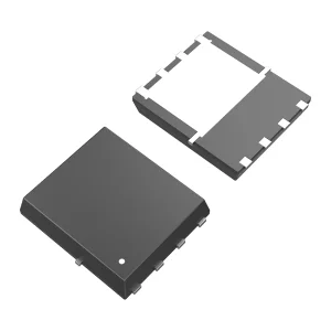
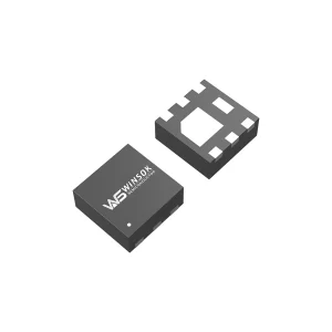
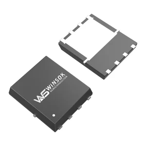
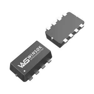
The consumer electronics ecosystem is undergoing a dramatic paradigm shift. Fast charging technologies, led by USB-C Power Delivery (PD 3.0/3.1) and custom OEM charging protocols, have transformed from luxury features into standard configurations. Modern designs demand capacities ranging from 20W up to 240W, compact topologies, and strict thermal envelopes. At the heart of these adapters are power semiconductors—primarily MOSFETs (Metal-Oxide-Semiconductor Field-Effect Transistors)—which dictate overall system conversion efficiency and density.
In the global market, sourcing stability and cost optimization are critical metrics. Design engineers and procurement managers face intense pressure to mitigate supply chain disruptions. The dependency on tier-one legacy brands like Infineon, STMicroelectronics, and ON Semiconductor often exposes manufacturers to long lead times. Consequently, finding a high-reliability, pin-to-pin, and parametrically equivalent MOSFET supplier is paramount. This technical whitepaper explores how advanced silicon optimization and packaging technologies allow second-source manufacturers to match or exceed OEM benchmark devices.
When qualifying secondary sources for fast charger applications (such as primary-side flyback switches, synchronous rectification, or VBUS load switches), engineers must perform strict comparison on key physical and electric parameters.
| Electrical Parameter | Critical Role in Fast Chargers | Matching Target Strategy for Equivalents |
|---|---|---|
| VDS (Drain-to-Source Voltage) | Prevents voltage spike breakdown during transient phases. | Must match or exceed the original OEM specification (e.g., 30V for synchronous rectification, 600V+ for primary switch). |
| RDS(on) (On-Resistance) | Determines conduction loss ($I^2R$). Critical for thermal management. | Equal or lower than target model under identical VGS conditions to avoid overheating. |
| Qg (Total Gate Charge) | Governs switching speed and drive losses. | Optimized equivalent Qg to prevent driver overloading and avoid electromagnetic interference (EMI). |
| Thermal Resistance (RθJC) | Ensures heat generated in the silicon junction dissipates into the PCB plane. | DFN5x6 or DFN3x3 package equivalents with exposed thermal pads are required. |
Our medium and low voltage N-channel and P-channel MOSFET lines focus on decreasing the specific on-resistance. Super-junction and split-gate trench technologies are used to achieve lowest-in-class RDS(on), minimizing continuous dissipation in high-amperage charger designs.
By optimizing the gate-to-drain and gate-to-source capacitance, our equivalent models allow fast switching transitions. This characteristic is particularly critical for Synchronous Rectification (SR) stages operating in CCM (Continuous Conduction Mode).
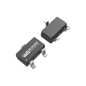
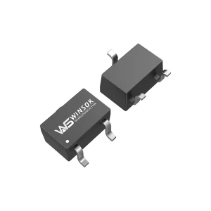
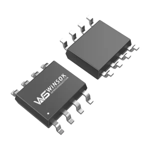
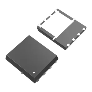
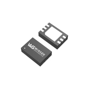
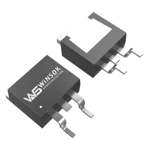
No redesign costs. Packages such as DFN3x3-8, DFN5x6-8, SOP-8, SOT-23, and TO-252 align with international standard outlines. This permits dynamic drop-in replacements during production cycles without PCB layout revisions.

HONGKONG Olukey INDUSTRY CO., LIMITED is a solution provider focusing on the overall solution of electronic product components. The main products mainly include: WINSOK MOSFET, Cmsemicon MCU, PCBA circuit board solution development and other three types of product lines.
At present, the products of Olukey Industry are widely used in automotive electronics, military electronics, smart industry, new energy, smart medical care, 5G, Internet of Things, smart home, and various consumer electronics products. Relying on the advantages of global general agents of major original factories, we are based in the Asia-Pacific market. Provide customers with various advanced high-tech electronic components by using comprehensive superior services, assist manufacturers in producing high-quality products and provide comprehensive services.
We use comprehensive high-quality services to provide customers with various types of advanced high-tech electronic components, assist manufacturers in producing high-quality products and provide comprehensive services. Over the years, the company has relied on reputation to survive, adhering to the tenet of "quality first, service first", and has established good cooperative relationships with many high-tech enterprises and original manufacturers at home and abroad.
Direct view into OLUKEY's sophisticated inventory management, production, and packaging logistics.




Relying on the advantages of global general agents of major original manufacturers, we are based on the Asia-Pacific market. Through active market development and effective resource integration, it has become one of the outstanding and fast-growing agents in the Asia-Pacific region. The company has many years of professional distribution experience. We use our comprehensive advantageous services to provide customers with various types of advanced high-tech electronic components, assist manufacturers in producing high-quality products and provide comprehensive services.
WINSOK MOSFET's product voltages are mainly medium and low voltage: 15V, 20V, 30V, 40V, 60V, 80V, 100V, 120V, 150V, 200V, 250V, 300V, 400V, 500V, 600V, 650V. The main packages include DFN3X3-8, DFN5X6-8, TO-252, TO-263, SOP-8, SOT-23, TO-220, etc. There are more than 600 models and more than 40 packages. Extensive coverage of medium-voltage and low-voltage MOSFET product lines on the market.
Cmsemicon MCU is a microcontroller company born in Shenzhen, with rich product types and technology research and development experience. Becoming a global high-value agent is the common goal pursued by OLUKEY Industrial employees. We adhere to the corporate values of "Pragmatism, Win-win, Service and Responsibility", continue to strengthen service quality, and aim to provide high-quality services. Work hand in hand with suppliers to jointly explore a larger market and contribute to the prosperity and development of semiconductors.


Depending on regional infrastructure, certification parameters, and regional power standards, fast-charger architectures utilize customized MOSFET topologies.
In China, Taiwan, and Southeast Asian manufacturing hubs, the emphasis is on compact, cost-effective 30W-65W single-port and multi-port phone chargers. Space is highly constrained, making DFN3X3-8 (like the WSD3090DN33 or WSD30L65DN33) and DFN2X2-6S packages highly favored due to their miniature footprint and solid transient thermal dissipation capability.
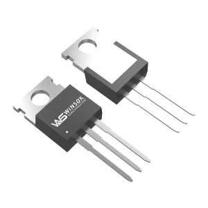
Targeting laptop charging protocols (65W to 140W+ USB-PD EPR) and industrial power adapters. These devices operate under rigorous thermal-limit requirements. Using low RDS(on) N-channel MOSFETs in DFN5X6-8 or TO-220-3L packages (such as equivalents to STL52DN4LF7AG or WSR140N10) ensures long operational lifetimes in continuous conduction modes.
Strict EMI and functional safety regulations demand robust dv/dt ruggedness. Here, dual N-channel or P-channel options (such as WSD2067DN32 and WSD2068DN23) are integrated as synchronous buck switches or input protection mechanisms to shield against load transients.
As charging architectures migrate toward higher switching frequencies, silicon MOSFETs are evolving alongside Wide Bandgap (WBG) technologies. In typical 65W to 100W power adapters, Gallium Nitride (GaN) transistors are increasingly preferred on the primary high-voltage side, while advanced Silicon MOSFETs remain the absolute standard for secondary Synchronous Rectification (SR) and VBUS load switching due to superior economic feasibility and robust parasitic protection.
WINSOK's technical roadmap addresses these developments by focusing on reduction of dynamic switching indices (Qgd / Qgs ratio) and implementing advanced packaging layouts to eliminate lead inductance. By minimizing package parasitical inductance, modern designs can push switching rates above 150kHz without generating voltage spikes that risk chip destruction.
Find answers to typical engineering, purchasing, and design integration questions regarding MOSFET equivalence.
Select models including low-voltage SOT, SOP, and high-power TO packages.

 Olukey