Engineered for ultra-low resistance, high avalanche tolerance, and superior thermal dissipation.
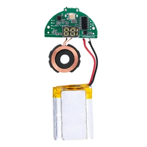
Lithium-ion and lithium iron phosphate (LiFePO4) battery packs represent the core energy reservoir for everything from consumer handheld tools to grid-scale energy storage systems. However, the chemistry of lithium cells demands rigorous oversight. A Battery Management System (BMS) acts as the electronic brain, protecting against overcharge, overdischarge, thermal runway, and short-circuit faults. Within this protective framework, the Power MOSFET functions as the critical high-speed gatekeeper.
By operating as high-efficiency switches, our OEM Power MOSFETs minimize voltage drops and thermal stress across the protection circuit modules (PCMs), increasing overall system efficiency and extending the life of the battery pack.

Delivering high-value, integrated hardware components for complex electronic systems.
HONGKONG Olukey INDUSTRY CO., LIMITED is a premier solution provider focusing on the overall integration and development of electronic product components. Our three primary product pillars include: WINSOK MOSFETs, Cmsemicon MCUs, and customized PCBA circuit board solution development.
Currently, our product lines are widely utilized in automotive electronics, military systems, smart industrial applications, new energy sectors, smart medical equipment, 5G architectures, the Internet of Things (IoT), smart home ecosystems, and high-performance consumer electronics. We are strategically based in the Asia-Pacific market, utilizing the logistical and supply chain advantages of global general agents representing major original factories.
Through our comprehensive, end-to-end integration, we deliver cutting-edge high-tech electronic components, helping global manufacturers build high-quality products from initial prototyping to massive scale-up.
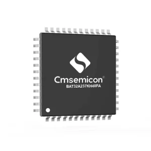
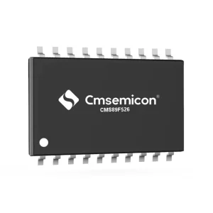
We work hand-in-hand with leading silicon foundries, assembly test facilities, and MCU developers (like Cmsemicon) to offer synchronized solutions where the processor, firmware, and power switches match optimally for minimal power loss.
Overcoming thermal and space constraints with optimized MOSFET packaging.
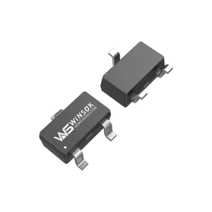
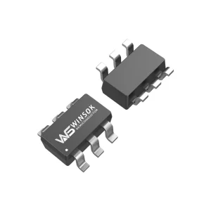
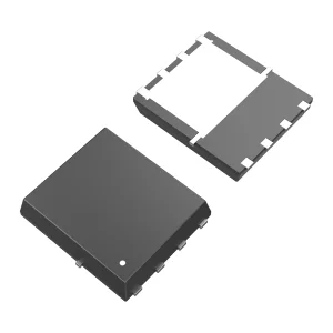
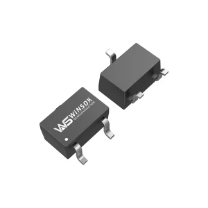
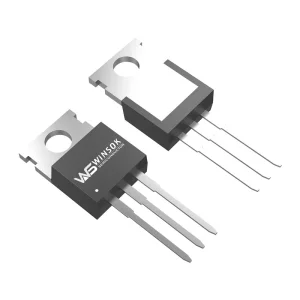
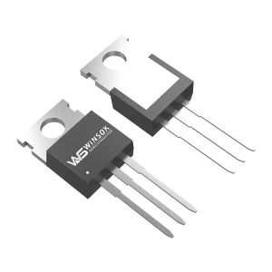
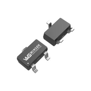
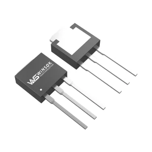
We provide over 40 packaging form factors including DFN3X3-8, DFN5X6-8, TO-252, TO-263, SOP-8, SOT-23, and TO-220. This allows engineers to optimize design layout density, reducing PCB footprint footprint by up to 40% using advanced DFN solutions.
WINSOK MOSFET voltage ratings span from low to medium ranges: 15V, 20V, 30V, 40V, 60V, 80V, 100V, 120V, 150V, 200V, 250V, 300V, 400V, 500V, 600V, and 650V. This covers everything from single-cell wearable packs to industrial multi-cell high-voltage arrays.
Through robust dynamic testing and continuous engineering improvements, our MOSFETs feature low reverse recovery charge (Qrr) and high avalanche ruggedness (EAS), preventing failure from voltage spikes.
Our Quality Philosophy: We use comprehensive, high-quality services to provide customers with advanced electronic components, assisting manufacturers in producing highly reliable products. Over the years, our company has built its reputation on the dual values of "Quality First, Service First", establishing deep cooperative relationships with high-tech enterprises and semiconductor original equipment manufacturers globally.
Why manufacturing and sourcing from China optimizes lead times, cost structure, and supply chain security.
The global semiconductor market demands agile production capabilities and short lead times. By leveraging our production hubs and general agency infrastructure in the Asia-Pacific region, we ensure robust inventory control and cost containment:





For international buyers and automotive/industrial OEMs, component sourcing is not just about price—it is about risk management, traceability, and global regulatory compliance.
Our complete MOSFET range meets strict environmental standards including RoHS and REACH directives, ensuring zero restricted hazardous substances. We maintain an ISO9001 certified quality management framework, providing production lot trace documentation with every order.
To reduce system integration risks, our design engineers offer technical support in target markets. We assist in cross-referencing industry standard parts, thermal modeling verification, and schematic reviews, helping reduce time-to-market for complex battery management applications.
Adapting advanced semiconductor switches to real-world battery conditions.
High-capacity battery packs in micro-mobility and light electric vehicles experience intense thermal shifts and high vibration. Our DFN5x6-8 and TO-220 packages provide low electrical resistance and high mechanical integrity, managing continuous discharge currents exceeding 100A safely.
Cordless power tools rely on transient high-current bursts. WINSOK medium-voltage MOSFETs feature high avalanche energy absorption ($E_{AS}$), allowing the system to resist inductive kickback spikes when motor loads stall.
Residential and grid solar energy storage systems run continuous charging cycles. In these systems, even fractional gains in efficiency lead to reduced operating costs. Our low conduction resistance MOSFETs keep thermal loads minimal, extending system lifetime without active cooling.
What lies ahead in the engineering of power switches and BMS integration.
As battery technologies push boundaries in charge density and charging speed, power semiconductors must evolve in parallel. Here are three primary trends reshaping the industry:
Traditional planar configurations are reaching their theoretical physical limits. By packing gate structures into vertical micro-trenches, we can decrease specific on-resistance ($R_{DS(on)} \times Area$) by over 30%, packing high current-carrying capacity into smaller footprints.
Modern battery architectures rely on tight communication between the power stage and the control loop. By pairing WINSOK MOSFETs with Cmsemicon 8-bit/32-bit MCUs, systems can monitor health parameters dynamically, enabling smart, adaptive safety margins.
As power densities increase, internal heat dissipation becomes the bottleneck. Package designs are shifting towards double-sided cooling and chip-scale packages (CSP). These technologies remove internal wire bonds, lowering package resistance and inductance, enabling high efficiency even under high-load profiles.

Expert technical answers to critical engineering and sourcing questions.
For a 10S pack (maximum charging voltage ~42V), we recommend a MOSFET with at least a 60V rating to provide a safety margin for inductive spikes. The on-resistance ($R_{DS(on)}$) should be as low as possible (typically <5 mΩ per device) to minimize heating during continuous discharge. Additionally, check the safe operating area (SOA) curve to verify the device can withstand short-circuit conditions before the BMS protection loop interrupts the current.
Because MOSFETs have an internal body diode, a single device can only block current in one direction. By wiring two N-channel MOSFETs back-to-back (source-to-source or drain-to-drain), the BMS can independently disable charging and discharging paths, preventing current flow in either direction when a fault occurs.
A lower gate charge ($Q_g$) allows the protection driver to switch the MOSFET on or off faster. In short-circuit scenarios, where current can spike to hundreds of amperes in microseconds, fast turn-off is critical to prevent thermal breakdown of the silicon and protect the cells.
Standard packages (such as SOT-23, TO-252, and DFN5x6) are regularly stocked, with delivery options available in 1-2 weeks. For customized silicon parameters or proprietary packaging designs, the prototyping phase typically takes 6-8 weeks, followed by full scale production after engineering validation.
High-performance silicon components, MCUs, and power solution modules.
 Olukey