High-performance silicon technologies optimized for harsh Middle Eastern environments, featuring extreme thermal dissipation and minimal conduction losses.
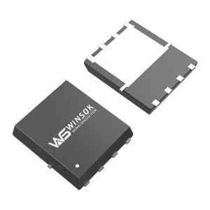
Ideal for Dubai Solar PV Micro-Inverters and Intelligent Telecom Power Systems.
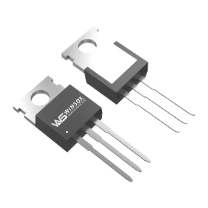
Robust package for Abu Dhabi Heavy Industrial Automation and Motor Control Units.
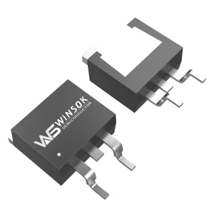
Engineered for Fujairah Port Marine Propulsion Systems and DC-DC Converters.
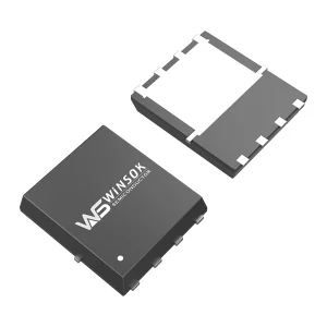
Compact dual-channel integration for Sharjah Smart City IoT Gateways and Node Systems.
Under the strategic goals of Operation 300bn and the UAE Net Zero 2050 charter, the nation is transitioning rapidly from an oil-dependent economic framework to a high-technology industrial powerhouse. This evolution demands robust power electronics capable of operating at elevated ambient temperatures without catastrophic derating. Dual Flat No-Lead (DFN) packaged MOSFETs represent a critical milestone in this shift.
Traditional packaging technologies, such as leaded TO-220 or DPAK configurations, present parasitic inductances and high thermal resistances that constrain performance in high-frequency switching circuits. Conversely, the DFN architecture eliminates lead frames, facilitating a direct solder path between the silicon die and the printed circuit board (PCB). This drastically reduces both thermal resistance ($R_{thJC}$) and source-inductance loops, permitting safe and efficient operation under the extreme thermal loads characteristic of the Arabian Peninsula.
Download UAE Technical Whitepaper
Consolidated data highlighting our production and distribution capacities across the GCC region.
In the field of power electronics, thermal dissipation is directly correlated with system reliability. In the GCC, where localized ambient temperatures within outdoor enclosures can exceed 60°C, typical silicon junctions can rapidly approach their maximum rating of 150°C. Modern DFN packages, such as the DFN3X3-8 and DFN5X6-8, utilize exposed thermal pads on the underside of the package body. This design allows the thermal impedance from junction to case ($R_{thJC}$) to drop below 1.0°C/W, which represents a massive improvement over leaded counterparts.
Furthermore, the package features an ultra-low profile, which reduces source-inductance. Parasitic inductance in gate-source loops can trigger spurious gate-source oscillations, risking self-turn-on and subsequent device destruction. By utilizing copper clip-bonding technology instead of traditional aluminum wire bonds, our DFN MOSFETs achieve a package resistance ($R_{DS(on)}$ contribution) close to zero, ensuring maximum system efficiency.
Maximizes efficiency by minimizing conduction losses, which is vital for high-current applications such as DC-DC converters and motor drivers.
Provides a direct thermal path to the PCB ground plane, allowing for rapid cooling even under high-load situations in hot desert climates.
Ready to meet the rigorous quality standards demanded by automotive electronics, military hardware, and critical aerospace projects.

HONGKONG Olukey INDUSTRY CO., LIMITED is an international, forward-thinking provider of comprehensive electronic component solutions. Our core product lines comprise WINSOK MOSFETs, Cmsemicon MCUs, and tailor-made PCBA circuit board developments. We serve industries that demand the highest levels of quality and consistency, including automotive electronics, defense, industrial automation, new energy systems, healthcare hardware, 5G networking infrastructure, and IoT smart home architectures.
By leveraging our strong partnerships with original equipment manufacturer factories worldwide, we provide the Asia-Pacific and Middle East markets with premier semiconductor options. Our foundational belief in "quality first, service first" guides our commitment to assisting manufacturers in producing reliable, energy-efficient products through every stage of development.
Discuss Your OEM/ODM ProjectsAligning advanced silicon characteristics with the region's primary industrial sectors.
1. Smart Grid & Renewable Integration: The UAE's solar energy infrastructure, exemplified by the massive Mohammed bin Rashid Al Maktoum Solar Park, requires high-efficiency power electronics to minimize conversion losses. DFN package MOSFETs are extensively utilized in grid-tied micro-inverters, maximizing power harvest.
2. Smart Buildings & LED Drivers: As Dubai and Abu Dhabi transition to green building standards, LED driver topologies must offer compact form factors. WINSOK DFN3X3-8 packages allow designers to implement ultra-slim drivers that run significantly cooler than legacy systems.
3. Industrial Automation & Oil/Gas Sector: Explosion-proof telemetry sensors and pipeline monitoring systems operating in remote desert environments require power management devices that remain stable under thermal swings. Our medium-voltage DFN products deliver high reliability over extended operating lifespans.

As silicon-based MOSFET technologies approach their physical limits, packaging innovation has become the primary driver of performance gains. The power semiconductor market is transitioning from wire-bonded packages to clip-bonded and 3D stack configurations. Over the next decade, the integration of Wide Bandgap (WBG) materials like Gallium Nitride (GaN) and Silicon Carbide (SiC) will accelerate; however, advanced Silicon (Si) MOSFETs remain the most cost-effective and reliable solution for systems operating under 200V.
Our technology roadmap focuses on reducing gate charge ($Q_g$) and reverse recovery charge ($Q_{rr}$). Lowering these values directly reduces dynamic switching losses in high-frequency converters. This is particularly important for server power supplies supporting the growing digital and AI data center footprint in the UAE.

Explore our catalog of advanced components designed for commercial and industrial applications across the Middle East.
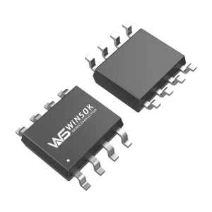
Ideal for UAE Smart Home Automation Hubs and Battery Protection Circuits.
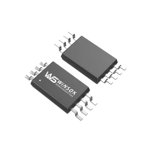
Compact design optimized for handheld consumer electronics and portable IoT nodes.

Supports high thermal loads in UAE EV Charging Wallboxes and BMS setups.
High-density switching for local telecom network hardware.

Highly reliable dual-rail management for commercial drone control systems.
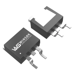
Rugged high-side switch for industrial Abu Dhabi oil refinery automation.

Robust thermal response for heavy motor control modules.
High-voltage, high-current switch for industrial power supplies.
Modern electronic design in the Gulf Cooperation Council (GCC) must address unique operational challenges. Ambient air temperatures within sealed enclosures regularly reach 50°C, and sun exposure can push internal device temperatures to 85°C before power consumption is even factored in. Designing systems to survive these conditions requires a holistic approach to engineering.
1. High-Performance Thermal Management
Using traditional thermal compounds in high-temperature environments can lead to dry-out and failure over time. We recommend combining our DFN MOSFETs with high-performance phase-change materials (PCM) or solid-state thermal pads. These options maintain contact stability across temperature fluctuations, preventing air gaps and helping the device operate within safe thermal margins.
2. Optimizing Gate Drive Circuits
To prevent switching losses at high frequencies, gate drive circuits must be carefully matched to the MOSFET's parameters. Using a low-impedance external driver helps control the gate charge ($Q_g$) quickly and cleanly, minimizing the time the transistor spends in its high-dissipation active region during switching transitions.
3. Component Selection and PCB Design
A robust power design relies on more than just the primary switching elements. We assist engineering teams by selecting complementary parts, including Cmsemicon microcontrollers and customized PCBA layouts, to ensure optimal performance. Placing bypass capacitors close to the MOSFET package pins minimizes voltage overshoot, protecting the system from high-voltage spikes.
Answers to technical questions regarding DFN MOSFET deployment and design optimization.
 Olukey


