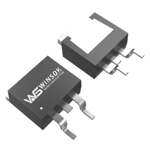
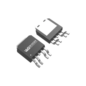
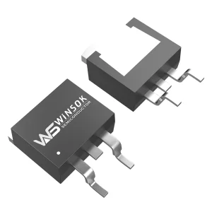
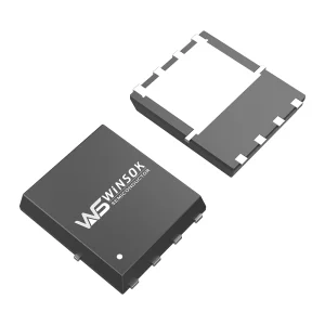
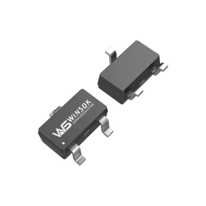
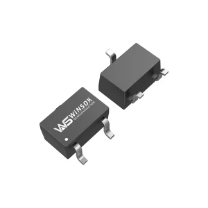
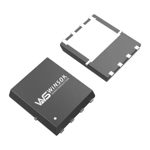
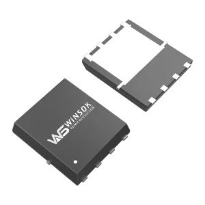
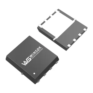
Explore high-efficiency N-Channel, P-Channel, and Dual MOSFETs designed to serve as footprint-compatible alternatives for fast charging and system power rails.
Technical insights into optimizing fast-charging topologies, mitigating thermal limits, and choosing high-availability replacement components.
The global expansion of USB Power Delivery (USB-PD), Quick Charge (QC), and universal adapter standards has forced consumer electronics design houses and industrial power designers to push thermal limits to their absolute thresholds. Fast chargers operating in the 65W to 240W spectrum demand power density margins that legacy silicon planar MOSFETs can no longer sustain economically.
By targeting critical parameters such as Gate Charge ($Q_g$), On-Resistance ($R_{DS(on)}$), and Reverse Recovery Charge ($Q_{rr}$), modern semiconductor alternatives allow design engineers to drop in replacement switches without redesigning gate-drive circuits or introducing electromagnetic interference (EMI) vulnerabilities.

"To scale power levels up to 240W under USB-PD 3.1 specifications without increasing power brick form factor, designers must implement synchronous rectification (SR) topologies. WINSOK’s selection of low-gate-charge, low-$R_{DS(on)}$ MOSFETs ensures switching transition periods are minimized, drastically mitigating heat generation and extending mean time between failures (MTBF)."
When specifying a replacement or alternative MOSFET vendor for OEM fast chargers, engineering managers look for performance parity. Below is an overview of how WINSOK's advanced Trench-gate and Superjunction architectures stand against standard industry requirements.
| Application Block | Required Parameters | WINSOK Direct Alternative Range | Key Packaging Formats |
|---|---|---|---|
| Primary Switch (High Voltage) | 500V - 650V | Low Qg | High dv/dt ruggedness | WSF / WST / WSM series (Medium to High V) | TO-220, TO-252, DFN5X6-8 |
| Synchronous Rectification (SR) | 40V - 100V | Sub-5mΩ RDS(on) | Low Qrr | WSK200N08, WSD50P10DN56, WSM340N10G | DFN5X6-8L, TOLL-8L, TO-263-2L |
| USB-PD Port VBUS Switch | 20V - 40V (N or P-Ch) | ESD Protected Gates | WST4040, WSD4023DN56, WST3032 | SOT-23, SOT-323, DFN3X3-8L |
| DC-DC Buck/Boost Stages | 30V - 60V Dual MOSFETs | Optimized thermal pad | WSD6035DN33, WSF4042 (N+P) | DFN3X3-8L, TO-252-4L |
The global power semiconductor market is currently undergoing a massive supply chain re-alignment. Geopolitical uncertainties, coupled with component allocation delays from Tier-1 European and North American chipmakers, have forced OEMs to seek out agile, localized design houses with robust distribution footprints in the Asia-Pacific hub.
Industrial clients across North America, the European Union, and Southeast Asia are standardizing reference designs that feature dual-sourced components from the start. Designing in dual-source options such as the WSK200N08 or WSM340N10G protects production pipelines against sudden factory shutdowns or lead time spikes. OLUKEY Industry's strategic distribution center in Hong Kong functions as a reliable hub that services global demand with minimal disruption.
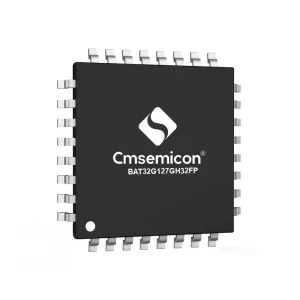
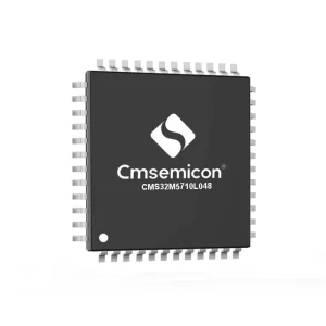
HONGKONG Olukey INDUSTRY CO., LIMITED is a comprehensive solution provider focusing on the overall integration and distribution of premium electronic components. Our dynamic product offering centers around three robust pillars: WINSOK MOSFET, Cmsemicon MCU, and custom PCBA circuit board solution development.
Currently, Olukey Industry's solutions are extensively adopted across high-reliability sectors including automotive electronics, defense and military electronics, smart industrial automation, new energy systems, smart medical diagnostic equipment, 5G baseband infrastructure, Internet of Things (IoT) nodes, smart home ecosystems, and high-performance consumer appliances. Relying on global relationships with leading original manufacturers, we support the Asia-Pacific and wider global markets, helping OEMs implement cost-effective, high-yield product designs.

Our core operating philosophy rests on "quality first, service first." Through rigorous supply chain auditing, electrical parameter characterization, and competitive packaging configurations, we provide high-availability drops that match or exceed original specifications.
WINSOK MOSFET voltage profiles cover: 15V, 20V, 30V, 40V, 60V, 80V, 100V, 120V, 150V, 200V, 250V, 300V, 400V, 500V, 600V, 650V. Standard packages include DFN3X3-8, DFN5X6-8, TO-252, TO-263, SOP-8, SOT-23, TO-220, and more, offering engineers over 600 specific models to target precise layouts. In conjunction with Cmsemicon MCU platforms—highly robust microcontrollers conceived in Shenzhen—we provide complete charging control, safety management, and communication interfaces in a single unified supply chain relationship.

How OLUKEY leverages the power of Shenzhen's semiconductor manufacturing cluster and Hong Kong's trade infrastructure.
By keeping fabrication, packaging, and wafer testing within the Greater Bay Area, we minimize transport latency and quickly react to silicon yield variations.
Our raw silicon wafer and epoxy molding compound sourcing channels are fully diversified, guaranteeing consistent output even during major raw material shortages.
Need a customized gate threshold voltage ($V_{GS(th)}$) or a non-standard thermal package? Our Shenzhen labs complete sample validation within short engineering cycles.

Our sub-micron manufacturing processes yield high cell density structures. This optimization delivers low static drain-source on-resistance, reducing thermal footprints within compact USB-PD wall plugs.

Every single wafer batch undergoes extensive electrical sorting, threshold measurement, and high-temperature reverse bias (HTRB) testing to confirm stable long-term performance under dynamic loads.
Power requirements vary significantly depending on localized electrical codes, average ambient temperatures, and regional regulatory frameworks:

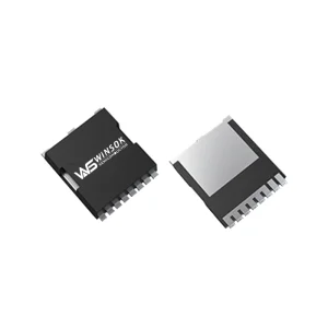
As charger power ratings move past 140W towards 240W, conventional packages like SOT-23 or standard TO-252 packages encounter physical space limitations. OLUKEY is actively helping clients migrate to ultra-thin, bottom-cooled packages like the TOLL-8L (e.g., WSM340N10G) and DFN2020 formats.
These new packages reduce board footprints by up to 60% compared to traditional D2PAK housings while improving thermal resistance by maximizing the leadframe contact area. The integration of high-speed drivers directly onto the PCB, combined with low-parasitic MOSFET switches, enables switching frequencies above 300kHz. This reduction in component size allows for smaller magnetic elements (transformers and inductors), ultimately shrinking the size of fast-charger adapters.
Every product distributed by OLUKEY Industry undergoes rigorous validation protocols to meet international standards. Our quality assurance framework aligns with strict environmental and safety directives:

Direct technical answers to the most common engineering and sourcing questions regarding fast-charger MOSFET alternatives.
High-reliability components optimized for auxiliary power rails, synchronous rectification, and smart communication circuits.
 Olukey