Switched-Mode Power Supplies (SMPS) form the cornerstone of modern energy conversion, requiring semiconductors that exhibit negligible power dissipation, fast switching transients, and robust thermal performance. In design scenarios such as LLC resonant converters, active clamp flybacks, and phase-shifted full bridges (PSFB), selecting the optimized N-channel or P-channel MOSFET directly influences system efficiency, power density, and EMI footprint.
Key parameters like low drain-source on-resistance (RDS(on)), low gate charge (Qg), and robust reverse recovery characteristics (Qrr) are essential. By reducing conduction and switching losses, engineers can design smaller cooling systems and magnetic components, paving the way for ultra-compact power bricks, server power shelves, and industrial DIN-rail modules.

HONGKONG Olukey INDUSTRY CO., LIMITED is a solution provider focusing on the overall solution of electronic product components. The main products mainly include: WINSOK MOSFET, Cmsemicon MCU, PCBA circuit board solution development and other three types of product lines. We deliver customized components engineered to function harmoniously within diverse topologies.
At present, the products of Olukey Industry are widely used in automotive electronics, military electronics, smart industry, new energy, smart medical care, 5G, Internet of Things, smart home, and various consumer electronics products. We utilize advanced design standards to guarantee performance in mission-critical environments.
Relying on the advantages of global general agents of major original factories, we are based in the Asia-Pacific market. We provide customers with various advanced high-tech electronic components by using comprehensive superior services, assist manufacturers in producing high-quality products and provide comprehensive services.
In modern industrial clusters across the Asia-Pacific, North American, and European regions, power density optimization drives market demand. Locally, WINSOK MOSFETs are deployed in high-capacity server farms (telecom and cloud database SMPS platforms), electric vehicle fast-charging networks, and photovoltaic micro-inverters. These applications leverage localized engineering support, ensuring compliance with layout requirements and regional grid regulations.
As power conversion trends transition toward higher switching frequencies, the coexistence of Silicon (Si), Gallium Nitride (GaN), and Silicon Carbide (SiC) is shaping technical roadmaps. WINSOK focuses on low and medium-voltage optimization to complement wide-bandgap primary topologies. Advanced gate charge (Qg) profiles allow our MOSFETs to function as high-frequency synchronous rectifiers alongside primary-side GaN power devices, offering balanced cost and performance.
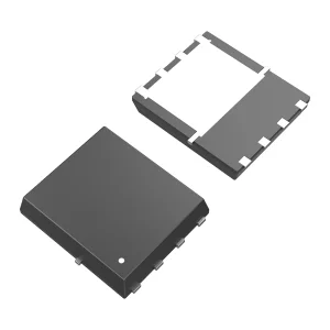
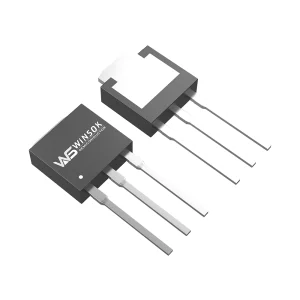
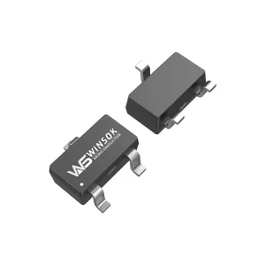
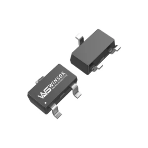
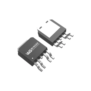
Future iterations of our SMPS MOSFET portfolio focus on minimized package resistance and inductance. Traditional leaded packages are shifting toward double-side cooled DFN5X6-8, DFN3X3-8, and compact SOT-23-3L form factors. These package configurations eliminate parasitic wire-bond inductance, reducing high-frequency ringing and EMI signature, while the top-side thermal pads facilitate heat rejection directly to chassis structures.
The semiconductor industry relies heavily on supply chain responsiveness and raw material security. Based in the heart of the Shenzhen-Hong Kong industrial semiconductor corridor, OLUKEY leverages access to major wafer foundries, assembly packaging lines, and rigorous test facilities. This proximity shortens engineering feedback loops and ensures predictable lead times, even during global allocation constraints.
Our strategic alignment with Cmsemicon MCU allows us to supply complete micro-controller and power stage solution pairs. By integrating design, packaging, testing, and shipping logistics into a unified ecosystem, we mitigate tariff risks, secure raw wafer buffers, and offer pricing stability to our industrial and automotive OEM partners.

Over the years, the company has relied on reputation to survive, adhering to the tenet of "quality first, service first", and has established good cooperative relationships with many high-tech enterprises and original manufacturers at home and abroad. By utilizing comprehensive, high-quality services, we provide customers with advanced electronic components, assisting manufacturers in producing reliable products.
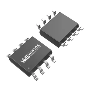
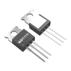
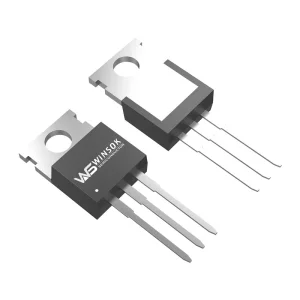
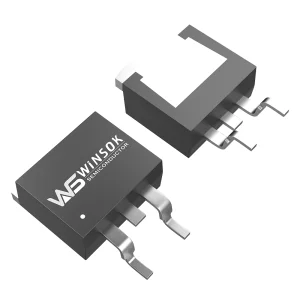
WINSOK MOSFET's product voltages are mainly medium and low voltage: 15V, 20V, 30V, 40V, 60V, 80V, 100V, 120V, 150V, 200V, 250V, 300V, 400V, 500V, 600V, 650V. The main packages include DFN3X3-8, DFN5X6-8, TO-252, TO-263, SOP-8, SOT-23, TO-220, etc. There are more than 600 models and more than 40 packages. This extensive coverage delivers versatility across medium-voltage and low-voltage MOSFET applications.
Cmsemicon MCU is a microcontroller company born in Shenzhen, with rich product types and technology research and development experience. Becoming a global high-value agent is the common goal pursued by OLUKEY Industrial employees. We adhere to the corporate values of "Pragmatism, Win-win, Service and Responsibility", continue to strengthen service quality, and aim to provide high-quality services. We work hand in hand with suppliers to explore larger markets and contribute to the development of the semiconductor sector.

Our quality management systems are designed to comply with international standards. From the wafer fabrication stage to final electrical parameter screening, our products undergo severe reliability tests. Key quality benchmarks include:

Our manufacturing and assembly partners maintain high standards of precision and automation. Equipped with high-speed die-attach, wire bonding, and automated sorting machines, the factory floor operates under strict environmental controls. Temperature, humidity, and airborne particulate levels are monitored continuously in class-10k cleanrooms.
This automated approach minimizes human intervention, reducing defects and variation. Each batch is serialized, allowing full traceability from the raw silicon ingot to the customer’s assembly line. These systems help us support our global clients with a reliable supply of power semiconductors.


 Olukey