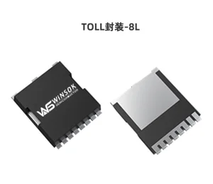
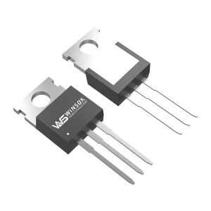
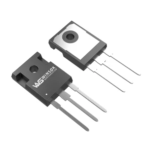
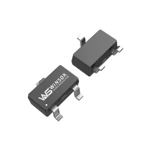
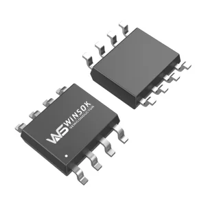
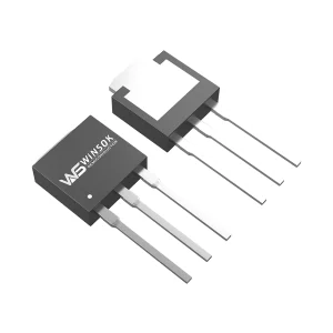
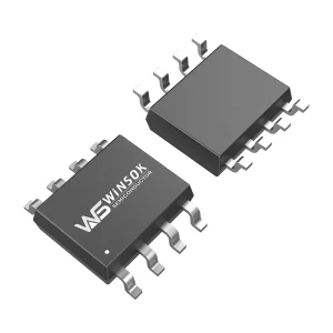
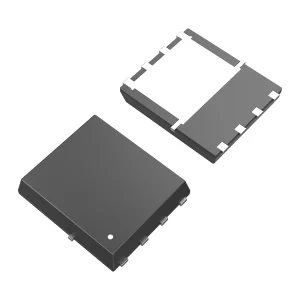
Below is our initial selection of high-performance MOSFETs configured for micro-inverters, string optimizer topologies, and auxiliary power circuits. Click to request samples for parametric cross-referencing and verification.


The rapid deployment of global solar photovoltaics (PV) has pushed power electronics design to its limits. In modern solar systems, the PV inverter stands as the central hub of energy transformation, converting variable direct current (DC) from solar panels into grid-compliant alternating current (AC). Inside these complex topologies—whether string inverters, micro-inverters, or central power conversion blocks—metal-oxide-semiconductor field-effect transistors (MOSFETs) act as the primary engines of power switching. High switching frequencies, high efficiency demands, and unforgiving environmental conditions require power semiconductors that offer maximum reliability and minimal losses.
"In the solar energy sector, system failures translate directly to lost revenue. Establishing a reliable, high-performance second-source cross-reference strategy for power MOSFETs is no longer just a purchasing backup plan—it is a critical strategy for engineering risk mitigation, supply chain stability, and cost optimization."
However, global supply chain disruptions, changing lead times, and rising component costs have forced hardware engineers and procurement directors to seek reliable replacement suppliers. Achieving a successful cross-reference is not simply about matching package outlines. It demands deep parameter matching—such as Drain-Source On-Resistance ($R_{DS(on)}$), Gate Charge ($Q_g$), Reverse Recovery Performance ($Q_{rr}$), Thermal Impedance ($Z_{\theta JC}$), and Safe Operating Area (SOA) boundaries. This guide explores the engineering, supply chain, and compliance aspects of sourcing high-performance replacement MOSFETs for solar applications.
PV inverter architectures rely heavily on specific semiconductor performance metrics at different stages of the power conversion chain. Sourcing replacement parts requires understanding how these topologies interact with individual MOSFET characteristics:
Maximum Power Point Tracking (MPPT) circuits raise the varying DC array voltage to a stable high-voltage DC bus. MOSFETs in this block operate at high frequencies (50kHz - 150kHz) to reduce inductor size. Key requirements: extremely low total gate charge ($Q_g$) and gate-to-drain charge ($Q_{gd}$) to minimize switching losses, combined with optimized $R_{DS(on)}$ to keep conduction losses minimal under high current loads.
For grid-tied micro-inverters, compact size is a primary design goal. Soft-switching topologies like Active Clamp Flyback require secondary-side synchronous rectification MOSFETs with rapid body-diode recovery. High reverse recovery charge ($Q_{rr}$) can cause high-voltage spikes and electromagnetic interference (EMI). Choosing a cross-reference with an integrated fast recovery body diode (FRD) prevents board-level failures.
In single-phase string inverters, H-bridge configurations are standard. During free-wheeling operational phases, the body-diode behavior of the MOSFETs is critical. Standard MOSFETs risk breakdown due to high dynamic $dv/dt$ stress. Replacement devices must feature rugged avalanche ratings ($E_{AS}$) and robust $dv/dt$ tolerance to guarantee continuous operation for more than 10 to 15 years.
Replacing a component directly with a cross-referenced device requires matching key electrical parameters. Below is a breakdown of the critical parameters our engineering team audits when validating a cross-reference replacement for a client:
| Electrical Parameter | Critical Engineering Metric | Impact on PV Inverter Design | Verification Target |
|---|---|---|---|
| Drain-to-Source Voltage ($V_{DSS}$) | Maximum breakdown voltage limit | Prevents failure from high line voltage transients | Ensure matching or higher ($V_{DSS} \ge Original$) |
| Static On-Resistance ($R_{DS(on)}$) | Ohmic resistance during conduction | Determines heat generation and conduction efficiency | Target matching or lower value ($\le 100\%$) |
| Total Gate Charge ($Q_g$) | Charge needed to turn on the gate channel | Affects gate driver current draw and switching speed | Aim for matching or lower to avoid driver overload |
| Body Diode Recovery Charge ($Q_{rr}$) | Charge cleared during diode turn-off | Key factor in synchronous rectification efficiency and EMI | Must match or exceed the speed of the original device |
| Thermal Resistance ($R_{\theta JC}$) | Heat transfer efficiency from junction to case | Determines system cooling requirements and component lifetime | Ensure equal or lower thermal resistance |
Over the past decade, China has built a comprehensive power semiconductor ecosystem, moving from simple assembly plants to high-end design, wafer fabrication, and packaging houses. Shenzhen and Hong Kong have emerged as key centers for this supply chain, offering significant advantages to global solar inverter manufacturers:
Western suppliers often quote lead times of 26 to 52 weeks during chip shortages. In contrast, Chinese factories backed by regional wafer foundries can deliver pre-production validation samples in 2 to 3 weeks and fulfill mass production orders within 6 to 8 weeks, helping manufacturers keep their production lines moving.
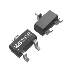
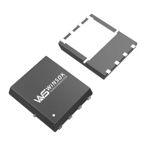
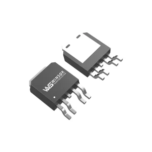
Our production facilities support a wide range of standard packages, including low-power surface-mount options (SOT-23, SOP-8) and high-current, low-inductance packaging (DFN3X3-8, DFN5X6-8, TOLLA-8L, TO-220-3L, TO-247, TO-263). This flexibility makes pin-to-pin drop-in replacements straightforward.
By using modern, automated sub-micron trench MOSFET processes and advanced packaging technologies, Chinese factories can deliver high-performance silicon at a lower cost than legacy Tier-1 brands. This helps inverter manufacturers improve their gross margins without sacrificing quality.
Deploying commercial, industrial, or residential solar installations requires complying with strict regional safety and environmental rules. Sourcing replacement semiconductors from an offshore partner requires strict compliance auditing. Our power components meet and exceed international standards:
Every MOSFET batch is certified under RoHS (Restriction of Hazardous Substances) and REACH regulations, ensuring hassle-free import and compliance for European and North American projects. We use halogen-free mold compounds to meet strict green energy manufacturing requirements.
Additionally, our factory processes follow ISO 9001:2015 for quality management and ISO 14001 for environmental management. For high-reliability sectors like solar tracking and automotive-grade EV charging systems, we offer product lines designed to meet AEC-Q101 standards, ensuring high-temperature reliability and excellent thermal cycling performance.
To bridge the gap between design teams and factories, our Hong Kong office acts as a centralized engineering and logistics hub. We provide direct access to application engineering support (FAE), comprehensive thermal simulation models (SPICE), and failure analysis (FA) reporting, ensuring rapid integration and validation on your boards.




HONGKONG Olukey INDUSTRY CO., LIMITED is an established solution provider focusing on the overall design and distribution of high-performance electronic components. Our three primary product lines include: WINSOK MOSFETs, Cmsemicon MCUs, and custom PCBA circuit board solutions.
We serve customers across automotive electronics, military electronics, industrial automation, new energy systems, smart medical hardware, 5G IoT networks, and consumer appliances. Leveraging our global partnerships and direct factory access, we support manufacturing clients in the Asia-Pacific region, Europe, and the Americas, helping them streamline procurement and improve overall system reliability.
Our WINSOK MOSFET product line covers low, medium, and high voltages: 15V, 20V, 30V, 40V, 60V, 80V, 100V, 120V, 150V, 200V, 250V, 300V, 400V, 500V, 600V, and 650V. With more than 600 models in over 40 industry-standard packages, we offer a comprehensive drop-in cross-reference matrix to help manufacturers maintain production continuity.
Selecting the right MOSFET is highly dependent on the design requirements of the specific target system. Here are typical use cases where our cross-reference components can be applied:
These compact units are installed directly behind individual solar panels, operating under extreme temperature swings. Low-voltage, high-current MOSFETs like the WSD30100DN56 (30V, 100A, DFN5X6-8L) and the WSC60N03 (30V, 60A, TO-251) are ideal for primary-side switching and secondary synchronous rectification, keeping heat generation low and eliminating the need for bulky heatsinks.
These systems run under high DC input voltages. High-current, medium-to-high voltage components, such as the WSL220N08 (85V, 210A, TO-247-3L) or the WSR170N04G (40V, 170A, TO-220-3L), are designed for multi-channel MPPT stages and high-voltage DC-DC converters, ensuring reliable long-term performance.
Modern home solar setups often integrate battery storage. Bidirectional battery charge/discharge circuits require low on-resistance MOSFETs to prevent thermal issues during high-rate charging. The WSM300N04G (40V, 300A, TOLLA-8L) offers a compact, high-current solution that reduces conduction losses in battery protection and distribution modules.
The PV inverter market is evolving rapidly, driven by the demand for higher power densities and smaller system footprints. While Wide Bandgap (WBG) materials like Silicon Carbide (SiC) and Gallium Nitride (GaN) are gaining traction in ultra-high-voltage central stations, Silicon (Si) MOSFETs remain the most cost-effective and reliable solution for residential and commercial systems below 1500V.
Modern silicon trench and superjunction technologies have significantly narrowed the performance gap, enabling lower on-resistance per unit area. This allows engineers to achieve high efficiency while keeping system costs down. By sourcing reliable second-source components, manufacturers can maintain a competitive edge and protect themselves from supply chain disruptions.
Explore our second selection of power components designed for high-efficiency switching, driver stages, and auxiliary circuits in commercial and industrial solar projects.
Our logistics and quality assurance operations run through modern hubs in Hong Kong and Shenzhen. Here is a look at our engineering, manufacturing, and distribution workflow:


Every batch of WINSOK MOSFETs undergoes rigorous testing to guarantee reliability. Our testing program includes:
By maintaining strict control over both manufacturing and testing, we deliver components that help solar inverter manufacturers build reliable, long-lasting products.

 Olukey